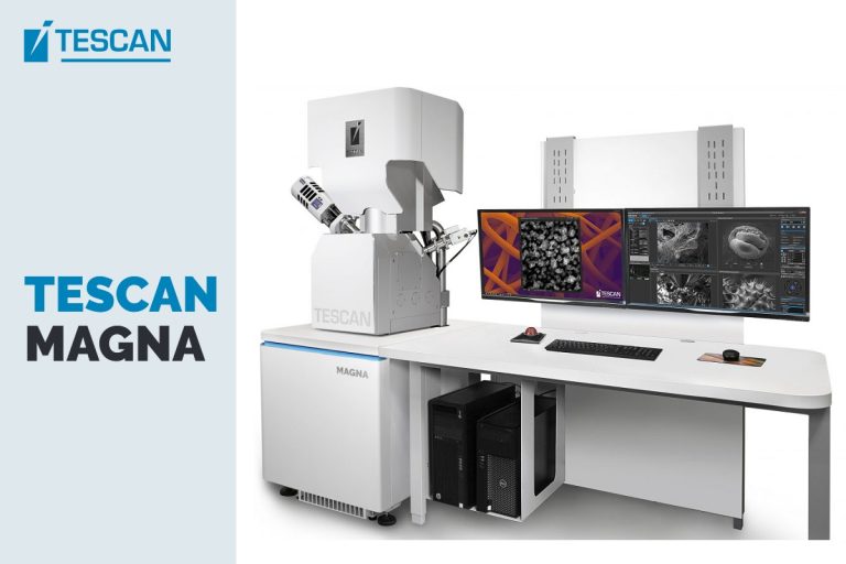
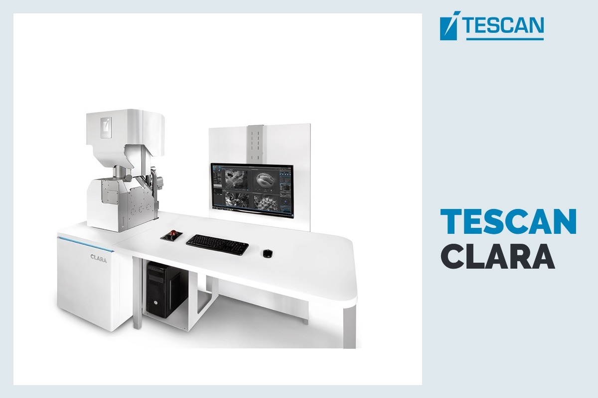
TESCAN CLARA for Materials Science
 Field-free analytical UHR SEM for materials characterization at the nanoscale.
The TESCAN CLARA UHR-SEM system is a scanning electron microscope (SEM) that meets the demands for high-quality images and microanalysis that regularly arise in various fields of research and technology.
TESCAN CLARA is powered by the TESCAN BrightBeam™ SEM column technology, which makes use of an integrated electrostatic-magnetic objective. This offers ultra-high-resolution abilities at low accelerating voltages in a field-free fashion—a crucial feature for no-compromise imaging of all types of samples, for example, those that are magnetic.
TESCAN CLARA is equipped with a special in-column multidetector system that enables preferable collection of electrons as per their take-off angle and energy. This leads to optimum topographic and compositional data from the sample. Equipped with a filtering grid, the multidetector provides access to filter BSE and SE energies selectively and improves materials contrast and the capability to live-switch between BSE and SE signal.
The axial detector, which is the second in-column detector, has been developed to gather SE signal at optimum efficiency and any landing voltages without tangible loss of SE signal. This renders UHR-SE observation very simple and regular, even at low landing voltages.
Moreover, TESCAN CLARA can be fitted with two In-chamber detectors and an E-T detector as a standard, to offer very high signal and topographical contrast from the sample. The optional retractable low energy BSE detector gathers wide-angle BSEs and offers high-material contrast, even at low accelerating voltages.
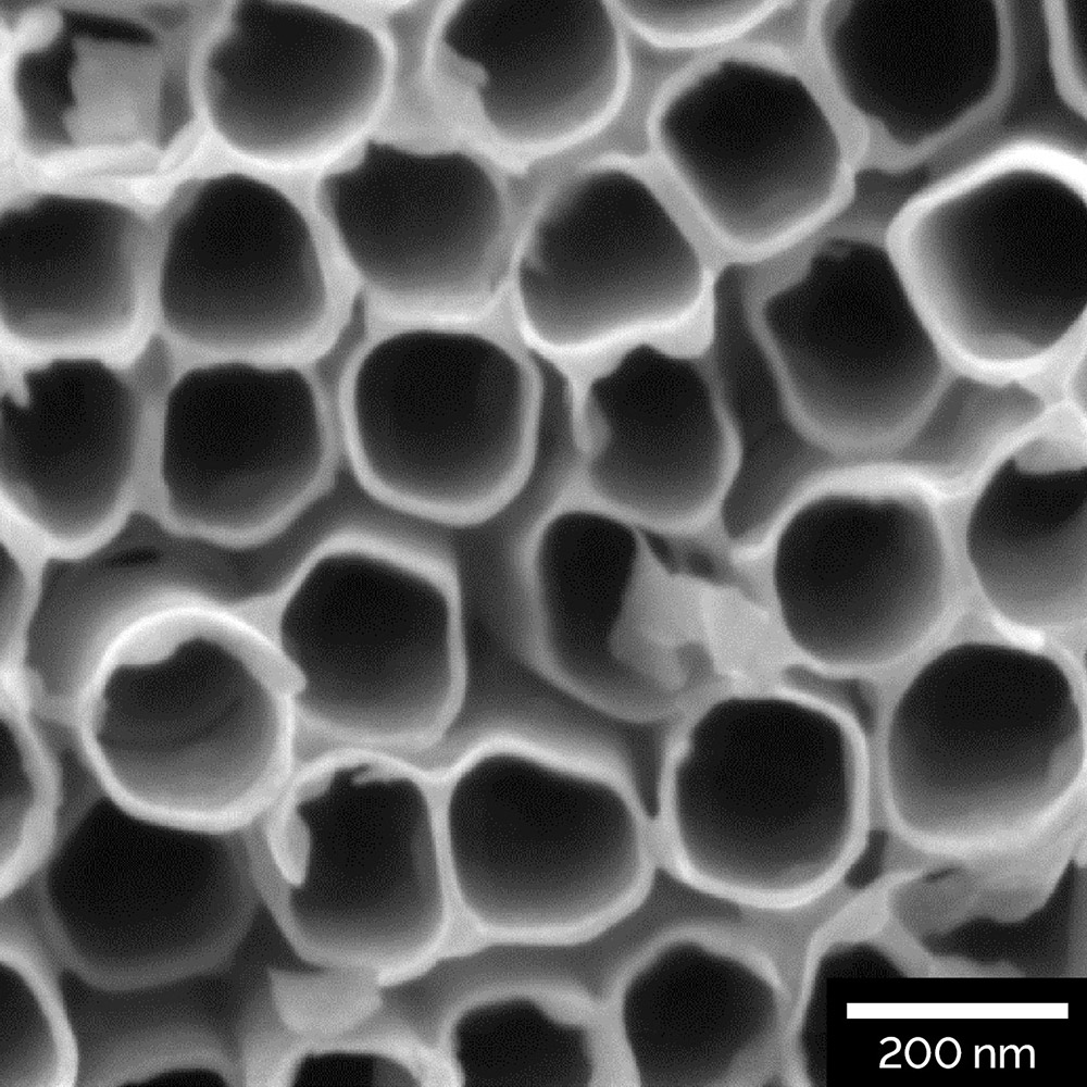
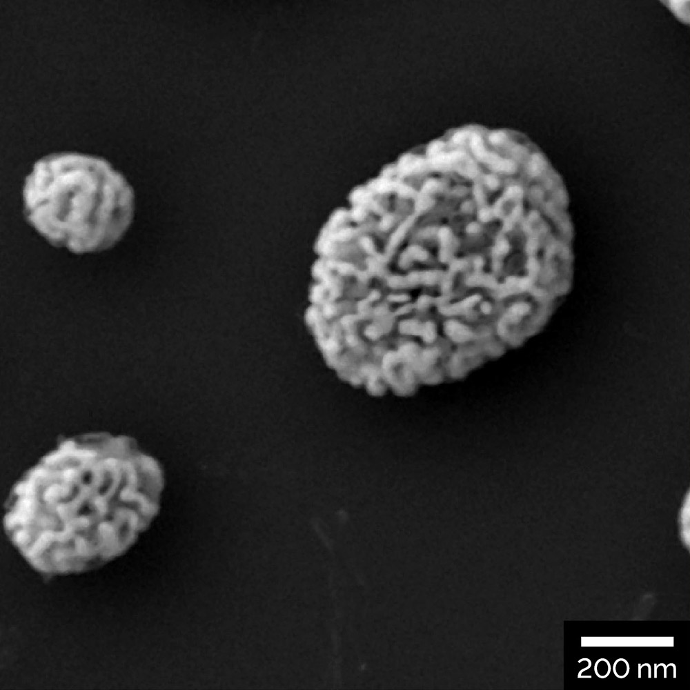
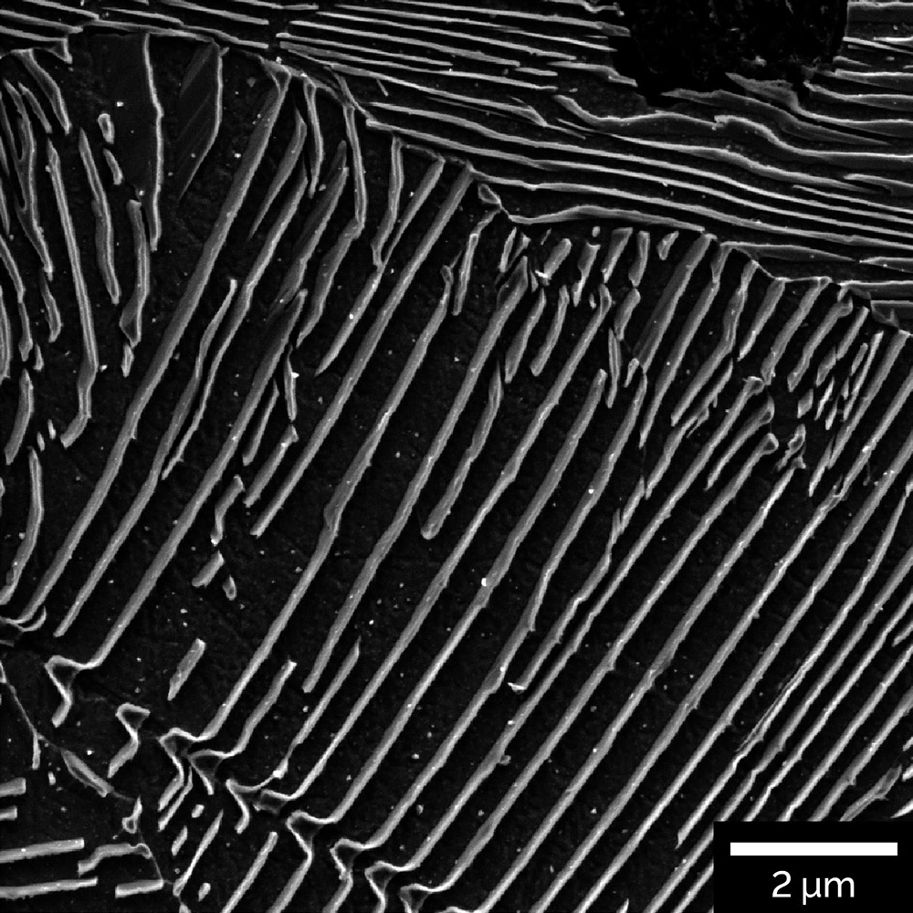
TESCAN CLARA is a truly flexible instrument and is perfect for the characterization of nanomaterials, severe quality control in the high-end manufacturing industry, as well as for Research and Development.