TESCAN MAGNA for Materials Science
UHR SEM for nanomaterials characterization at sub-nanometer scale. TESCAN MAGNA is a sum up of Ultra-high resolution and high-contrast imaging of next-gen materials with a…
Scanning Electron Microscopy has become an essential tool for materials science and engineering.
TESCAN offers an extended portfolio of turnkey systems, tailored to help scientists and researchers in materials science make progress and achieve their goals. TESCAN’s broad range of dedicated and innovative instruments is part of our firm commitment to push materials science forward.
Find SEM Solutions for Materials Science below :
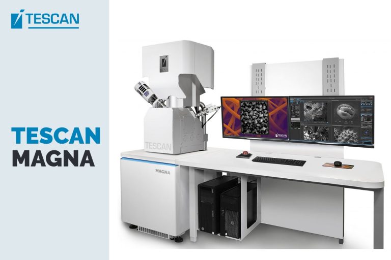
UHR SEM for nanomaterials characterization at sub-nanometer scale. TESCAN MAGNA is a sum up of Ultra-high resolution and high-contrast imaging of next-gen materials with a…
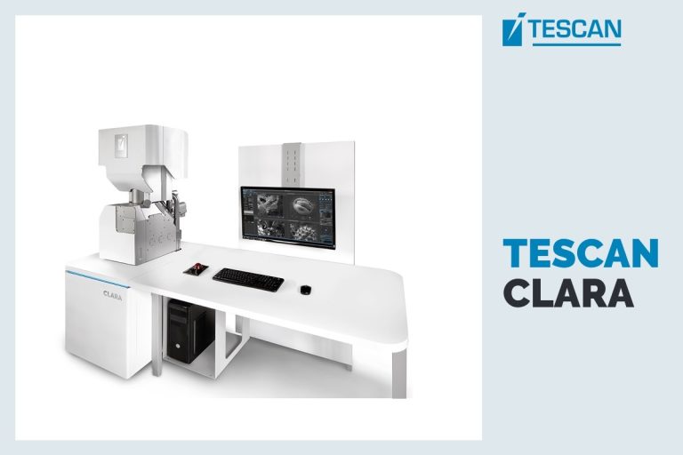
Field-free analytical UHR SEM for materials characterization at the nanoscale. The TESCAN CLARA UHR-SEM system is a scanning electron microscope (SEM) that meets the demands…
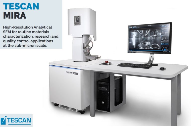
High-resolution analytical SEM (Scanning Electrone Microscope) for routine materials characterization, research and quality control applications at the sub-micron scale. TESCAN MIRA’s 4th generation Scanning Electron…
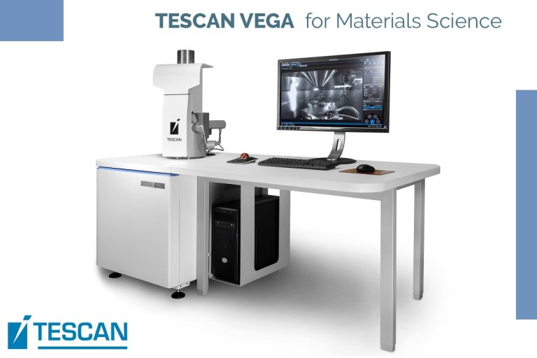
Analytical SEM for routine materials characterization, research and quality control applications at the micron scale. TESCAN VEGA’s 4th generation Scanning Electron Microscope (SEM) with tungsten…
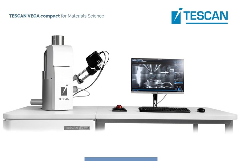
Compact analytical SEM (Scanning Electron Microscope) for routine materials characterization, research and quality control applications at the micron scale. Proving that entry-level doesn’t have to…