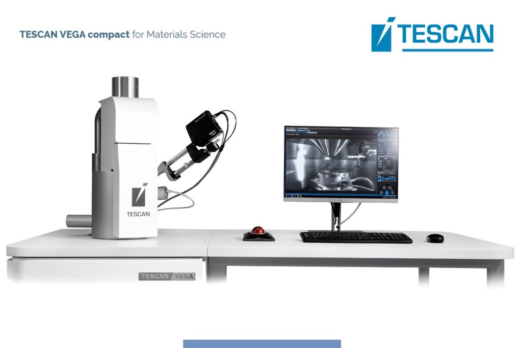
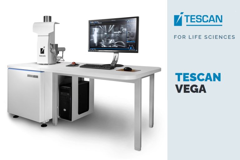
TESCAN VEGA Compact for Materials Science
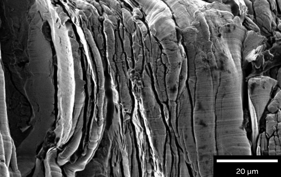
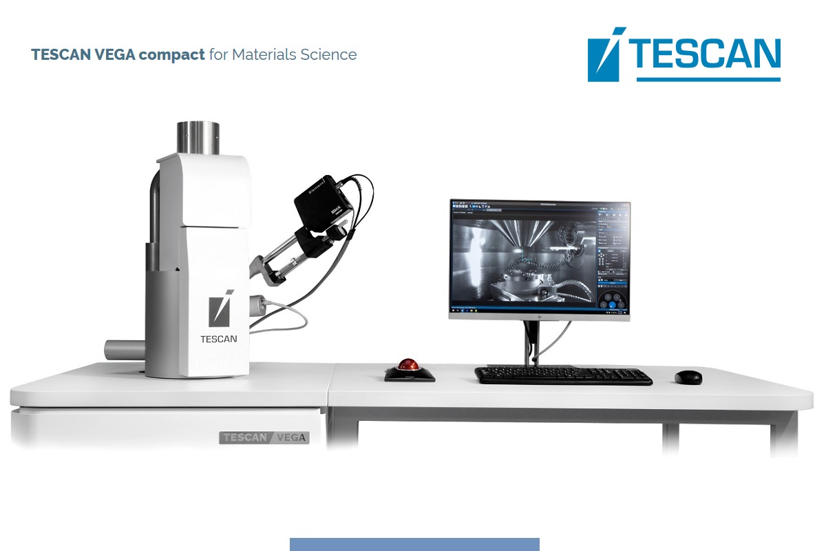 Compact analytical SEM (Scanning Electron Microscope) for routine materials characterization, research and quality control applications at the micron scale.
Proving that entry-level doesn’t have to mean compromising on results, TESCAN VEGA Compact offers a complete analytical SEM solution for laboratories that place a priority on both easy operation and quick time to high quality images and compositional (EDS) analysis.
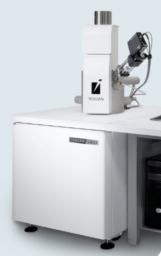
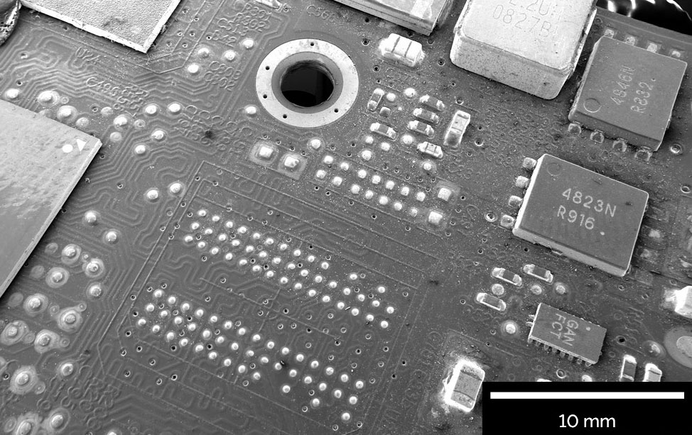
TESCAN VEGA Compact features a simplified configuration that includes only the most critical components for efficiently capturing morphological and elemental data, allowing TESCAN VEGA Compact to occupy a smaller footprint in the lab. With the ability to accommodate large-sized samples that are common in industry, materials science and semiconductors — like metallurgical cross-sections, welded structures, or printed circuit boards – TESCAN VEGA Compact is a great choice for not only your current materials inspection, quality control and failure analysis needs, but also your future analytical needs.
TESCAN VEGA Compact operates from TESCAN’s own full-featured graphical user interface, TESCAN Essence™, which is at the heart of all TESCAN SEM and FIB-SEM instruments. An operator who learns on TESCAN VEGA Compact can easily make the transition to other TESCAN microscopes or adapt some features of the Essence software environment to match the GUI of other instruments in the lab.